The research projects of the group fall within two main categories: electro-optic devices and fiber optics.
1. Electro-optic devices: active, hybrid silicon-photonic devices
Our interest in electro-optic devices is primarily focused on silicon photonics: the incorporation of photonic functionalities, such as the generation, modulation, guiding, filtering and detection of light, within the silicon material platform. The traditional argument in favor of silicon photonics is based on its compatibility with the mature silicon integrated circuits (IC) manufacturing. Silicon wafers have the lowest cost (per unit area) and the highest crystal quality of any semiconductor material. The industry is able to produce micro-processors with billions of components, all integrated into a thumb-size chip, and offer them at such a low price that they appear in consumer electronics. Silicon manufacturing represents the most spectacular convergence of technological sophistication and the economics of scale. Creating low-cost photonics for the mass market applications by exploiting the mighty IC industry has been the traditional motivation for silicon photonics researchers.
There are several potential advantages to using silicon for photonic purposes. Silicon is boasting a low-propagation-loss window, extending from the wavelength of 1.1 μm to nearly 7 μm (see Fig. 1.1 below). This transparency window includes the all-important telecommunication wavelengths of 1.3 μm and 1.55 μm, and also the middle-infra-red region that has many sensing and imaging applications. Silicon has a superior thermal conductivity, compared to most other photonic materials. The optical damage threshold, denoting the optical intensity for which the material is permanently damaged, is an order of magnitude higher in silicon compared to GaAs, for example. In addition, silicon on insulator (SOI) wafers offer a particularly large contrast index, between that of silicon (n = 3.45) and that of SiO2 (also known as silica, n = 1.45). This index contrast leads to particularly tight confinement of the modal intensity, which scales down photonic devices to hundreds of nanometers level. The above properties make silicon an excellent candidate for the implementation of passive optical devices.
The role of silicon is more complex in active photonic devices. These include critical components such as light sources in the forms of light-emitting diodes (LEDs) and laser diodes, semiconductor optical amplifiers (SOAs), electro-optic modulators which imprint information upon a continuous optical field, and detectors. Silicon suffers from fundamental drawbacks which keep it from realizing few of these functionalities in a straight-forward manner. For example, silicon is a poor converter of electrical current to light due to its indirect bandgap, a deficiency which makes the realization of silicon light sources very challenging. Also, the electro-optic effect which underlies the operation of modulators in several other materials is practically absent in silicon.
The primary objective of much of our work in silicon photonics is to try and overcome the material deficiencies of silicon in active photonic devices using hybrid integration of additional materials on the silicon platform. The vertical integration approach relies on wafer bonding between SOI wafers and active electro-optical materials. Specific research projects include:
1.1 Enhanced wafer bonding based on self-assembled organic monolayers
Low-temperature wafer bonding has proven to be a useful approach for making devices that combine GaAs or InP with silicon. Bonding in these devices relies on Van-der Waals forces and hydrogen bonds between oxidized surfaces, or on relatively thick matrices of polymers such as BCB. The former is a challenging process of low yield, whereas the latter provides a thick and poorly reproducible interface.
Our group, together with the group of Prof. Chaim Sukenik of the Chemistry Department, is pursuing an alternative bonding technology that is based on using organic thin films to modify the surfaces of the wafers to be bonded and promote a bonding approach based on a continuous chain of covalent bonds bridging the two wafers. Such bonding brings several unique advantages to the CMOS-integrated photonic platform:
- Covalent bonds are considerably stronger than the inter-molecular forces used in ‘direct’ bonding to-date. Therefore, a significant improvement in yield is anticipated. Consequently, the cost of hybrid silicon/InP devices can be reduced.
- The organic interface between the wafers can be made ultra-thin. Such a bonding layer would help circumvent heat-dissipation issues that plague bonding approaches involving thicker polymer matrices.
- The reactivity of the organic layers can be patterned to allow for area-selective bonding of devices of different materials at different locations above a passive silicon-photonic layer.
This research project is supported in part by the Israeli Science Foundation (ISF), 2010-2014.
1.2 Hybrid, InGaAsP/Si integrated laser and modulator structures
A monolithic integration of laser sources together with high speed, silicon integrated electronic circuits has been highly sought after in the electro-optics research community for decades. Recent years witnessed a major reawakening of the interest in Si-integrated lasers, pursued primarily to support high rate, inter-chip and intra-chip communication within large scale multi-processor computers. One particularly successful approach towards realizing these lasers is based on wafer bonding of AlGaInAs material on top of a pre-patterned Si-on-insulator (SOI) wafer. This approach was proposed and beautifully demonstrated by the group of Prof. John E. Bowers at the University of California at Santa Barbara, in collaboration with Intel. The geometry of the bonded structure is designed to support a joint optical mode, whose profile overlaps both materials. Using this underlying technology, the AlGaInAs layers, which include multiple quantum wells (MQWs), are patterned post-bonding to produce various laser geometries, the outputs of which are predominantly emitted form the underlying Si waveguides.
During his post-doc stay with the group of Prof. Amnon Yariv in Caltech, Dr. Avi Zadok and his colleagues adapted a similar platform and demonstrated hybrid Si/III-V, Fabri-Perot (FP) lasers based on a different III-V material system, i.e. InGaAsP quaternary compounds. They found that the threshold current density and the threshold voltage of the fabricated devices are 30-40% lower than those of the corresponding, previously reported FP devices. At the same time, the output power and differential slope efficiency of the devices are both higher than previously reported. This research effort was carried out jointly with Dr. Xiankai (formerly with the Yariv group, currently a post-doctoral fellow at Yale), Dr. Michael Shearn (formerly with Prof. Axel Scherer’s group) and Dr. Kenneth Diest (who was with Prof. Harry A. Atwater’s group). The results were presented in an Optics Letters paper of May 2009 (Full text).
Our research efforts in this area target the design, fabrication and characterization of hybrid silicon/III-V lasers of improved efficiency, and hybrid silicon/III-V modulators for advanced modulation formats.
The project is funded in part by the Israeli Chief Scientist Office within MAGNET program ‘Tera Santa’: 2010-2013.
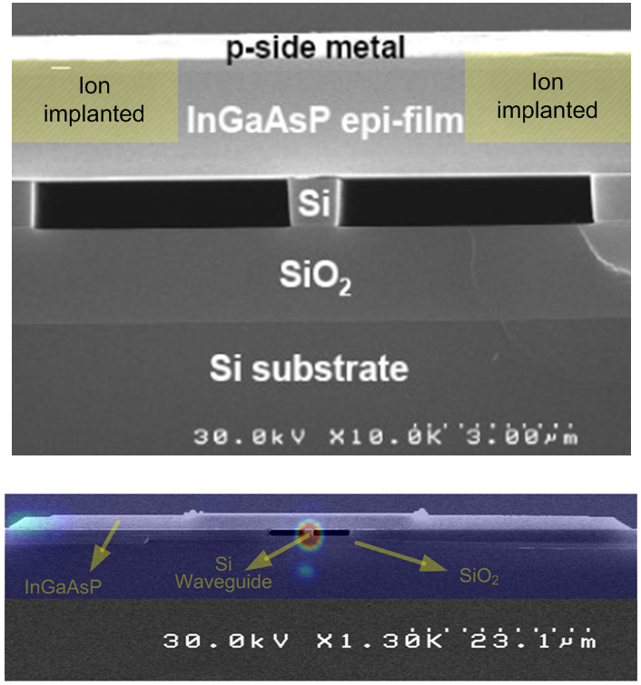
SEM Device cross-section (top), with a superimposed, scaled image of the emitting facet indicating confinement of the output an Si waveguide (bottom)
1.3 Hybrid silicon/LiNbO3 integration
LiNbO3 is the material of choice in most optical modulators that are based on the electro-optic effect. Effective vertical integration of LiNbO3 and SOI waveguides could allow for silicon-integrated electro-optic modulators. In this project, wafer bonding techniques are used for the vertical integration of the two materials, and the demonstration of active, hybrid devices.
The research project is funded in part by the Israeli Ministry of Defense and Civan Technologies Ltd of Jerusalem, Israel.
1.4 Planar light-guide circuits for the optical wavelet division multiplexing
Modern optical communication networks are constantly striving to improve their spectral efficiency (in bits/sec per Hz bandwidth). One particular scheme for multiplexing a large number of data streams that has been drawing increased attention is that of optical wavelet division multiplexing or OWDM. Rather than a specific time slot or spectral range, a specific wavelet shape is assigned to each OWDM user. The orthogonality of the set of wavelet functions allows for the successful demultiplexing of the different streams at the receiver end. OWDM has several potential advantages over the more widely-recognized optical frequency domain multiplexing (OWDM), such as a better tolerance to nonlinear impairments and a lower computational complexity of the digital wavelet transform.
The objective of the research project is to develop passive, planar light-guide circuits (PLC) in SOI for the all-optical implementation of the discrete wavelet transform. An all-optical implementation could relieve the bottle-neck of high rate digital signal processing that is necessary for the computation of the transform at high data rates. The optical-wavelet PLC could be later combined with hybrid silicon/InP modulators to provide an integrated transmitter.
The project is funded in part by the Israeli Chief Scientist Office within MAGNET program ‘Tera Santa’: 2010-2013. The research is carried out in collaboration with Optiway company of Rosh-Ha’ayin, Israel.
2. Fiber-optics research activities
Our research projects in fiber optics are related to optical communication, distributed sensing and microwave photonics
2.1 Brillouin optical time domain reflectometry distributed sensing with enhanced range and resolution
Brillouin Optical Time-Domain Reflectometry (B-OTDR) is a fiber-optic sensing technology which allows for the distributed monitoring of temperature and mechanical strain. Such measurement is critical in the structural health monitoring and the preventive maintenance in the geo-synthetic and transportation industries. The resolution of commercially available B-OTDRs is on the order of meters, and their range reaches a few tens of km. High resolution typically requires short pulses, whereas a long measurement range necessitates longer pulses. Hence, there is an inherent trade-off between range and resolution. Such trade-offs are familiar to those working on radar systems, that face similar restrictions. Through seventy years of research, the radar community came up with numerous ingenious solutions for pushing the systems performance envelope. Thus far there has been little penetration of radar-originated techniques to the realm of B-OTDR sensing. The incorporation of more elaborate signal processing and pulse shaping techniques could enhance BOTDR resolution to the cm range, or extend the measurement range towards 100 km. If the strain profile is more spatially accurate, the evaluation of the stress (proportional to the strain derivative) becomes more accurate as well. Measurement techniques to be considered include, but are not restricted to, frequency sweeping of the Brillouin pump and signal waves, and amplitude or frequency domain coding with matched detection.
The research is carried out in collaboration with the groups of Prof. Luc Thevenaz of EPFL, Switzerland, and Prof. Moshe Tur of Tel-Aviv University.
2.2 Polarization attributed of stimulated Brillouin scattering in long standard fibers
Stimulated Brillouin scattering (SBS) is a nonlinear optical interaction between a pump wave, and a typically weaker, counter-propagating signal wave. The threshold power of SBS is the lowest of all nonlinear propagation effect in silica optical fibers. The local SBS interaction, at a given point along an optical fiber, is maximal when the state of polarization (SOP) of the pump is aligned with that of the signal, and it vanishes if the two SOPs are orthogonal. In standard single mode fibers, the overall SBS signal amplification (or attenuation) depends on the birefringence properties of the fiber, as well as on the input SOPs of both the pump and the seed signal waves. As SBS is studied intensively for applications such as fiber lasers, distributed sensing and slow light, a thorough examination of its polarization properties is of large relevance.
In this work, the SBS amplification of an arbitrarily polarized input signal in a randomly birefringent fiber is examined, as well as the role of SBS in the evolution of the signal SOP. The analysis includes Stokes and anti-Stokes waves. A propagation equation for the signal SOP is formulated and analyzed, in Jones and Stokes spaces. In particular, it is found that the output SOP of an SBS amplified Stokes wave in a standard, single mode fiber is drawn towards the complex conjugate of the input pump SOP. On the other hand, the output SOP of the residual, attenuated anti-Stokes signal is repelled from the same SOP. These findings are supported by simulations and experiments. The results are applicable to random SOP synthesis, coherent detection of fiber sensors, advanced modulation formats and implementations of optical filters. Finally, we find that SBS-based ‘slow light’ setups display polarization mode dispersion (PMD).

SBS power amplification of the Stokes probe wave for different input states of polarization: maximum gain (blue), minimum gain (green), and ‘near-minimum’ gain (red). (a): Stokes wave. (c): anti-Stokes wave. (b), (d): Poincare sphere representation of output polarization pulling of Stokes and anti-Stokes probe waves, respectively. Click on the image for the Full Text.
2.3 Photonic generation of ultra-wideband noise waveforms and their applications
Ultra-wideband (UWB) communication provides several potential advantages over traditional, narrowband formats: improved immunity to multi-path fading, increased ranging resolution, large tolerance to interfering legacy systems, enhanced object penetration and more. UWB technology is being considered in a myriad of applications, including high-speed internet access, sensor networks, high accuracy localization, precision navigation, covert communication links and radars, through the wall imaging and ground penetrating radars. Interest in UWB communication had picked up considerably since 2002, when the US Federal Communication Committee (FCC) allocated the frequency range of 3.6-10.1 GHz for unlicensed, indoor wireless UWB communication. The FCC standard imposes several limitations on the transmitted signals. First, the power spectral density must comply with complicated spectral masks. In addition, the signal power is severely restricted, limiting the range of UWB indoor wireless transmission, for example, to only 10-15 m. In many cases, a UWB radio-based system would have to complement wireless transmission by other distribution means, and optical fibers would be the medium of choice for high-frequency signals. With radio-over-fiber integration on the horizon, the generation of the UWB pulses by photonic methods becomes attractive.
Most microwave-photonic UWB generation schemes thus far target impulse radio implementations: the transmission of tailored short pulses and their coherent detection. UWB architectures that are based on impulse radio require elaborate pulse shaping and a detailed knowledge of the communication channel properties. A possible alternative is the transmission of modulated, broadband noise waveforms. The objective of the research project is the generation of UWB noise, based on the amplified spontaneous emission associated with stimulated Brillouin scattering in fiber (SBS-ASE). SBS-ASE noise generation allows for an agile reconfiguration of the central radio frequency (RF), bandwidth and PSD. The generated waveforms are applicable to noise-based broadband radars as well.

Left – experimental setup for the generation of transmit-reference UWB noise waveforms based on SBS-ASE. Right – experimental modulated noise without (top) and with (center) transmitted reference, and transmit reference waveform auto-correlation (bottom). Click on the image for the Full Text.
The project is carried out in collaboration with the group of Prof. Moshe Tur of Tel-Aviv University. The work is funded in part by the German-Israeli Foundation (GIF).
2.4 Photonic implementation of true-time-delay for optical beam forming in radars
Variable delay of analog signals in radar systems is a promising potential application for photonic processing. In these systems, the directional stirring of the transmitted beam is achieved through control of the delay between the signals feeding neighboring elements, in an array of antennas. The delay lines used must accommodate broadband signals with stringent distortion tolerances. Photonic processing implementations are appealing due to their very large usable bandwidth, low frequency-independent loss, immunity to electromagnetic interference, and parallelism through wavelength multiplexing. In this research project, we aim at reaching an all-optical, continuously variable delay of up to 50 nsec, for broadband radar pulses of arbitrary carrier frequencies.
2.5 Mitigation of nonlinear impairment in wavelength-division multiplexed coherent optical communication
Since the inception of optical communication thirty years ago, the transfer of data over optical fibers had relied on binary intensity modulation and direct detection (IM-DD) almost exclusively. The IM-DD format allows for conceptually simple transmitters and receivers, which do not require phase information. On the other hand, IM-DD transmission does not use the bandwidth resource effectively. In addition, the loss of phase information upon detection restricts the mitigation of linear optical impairments, such as chromatic dispersion or polarization mode dispersion, by means of digital signal processing.
Recent years had witnessed a major revolution in optical communication systems. As available bandwidth becomes scarce in our era of the internet, more elaborate, spectrally efficient modulation formats are quickly being adapted by the industry. These formats, such as differential quadrature phase shift keying (D-QPSK) or multi-level quadrature amplitude modulation (QAM), make use of both optical amplitude and phase to carry more than one bit of data per symbol. Further motivation is provided by the availability fast analog-to-digital converters (ADCs) and parallel processors of unprecedented operation rates, which enable electronic post-compensation of optical impairments with sufficient throughput. These dramatic developments do not come without a cost: relatively complex coherent receivers are necessary for decoding the optical phase, and higher signal to noise ratios (SNR) are required for proper demodulation. Despite these challenges, the state of the art in high-rate, long-distance coherent optical communication does not halt.
Many concepts of coherent transmission and detection are being adapted and transferred from the realms of cellular and wireless networks into optical communication. However, certain attributes of the optical fiber are markedly different from those of other propagation media. In particular, the propagation of multiple optical channels over thousands of km is highly nonlinear: the refractive index of the fiber is intensity dependent, due to the third-order nonlinear Kerr effect. The Kerr effect manifests in four-wave mixing (FWM), self-phase modulation (SPM) and cross-phase modulation (XPM) phenomena, which alter both the amplitude and the phase of propagating waveforms. Coherent communication is susceptible to nonlinear phase modulation impairments, due to the role of the optical phase as the bearer of information.
In this research project, we look to propose and demonstrate computationally efficient schemes for the electronic mitigation and compensation of nonlinear propagation impairments in multi-channel, coherent optical communication networks.