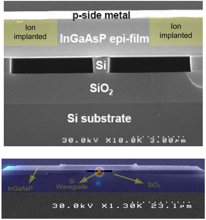
SEM Device cross-section (top), with a superimposed, scaled image of the emitting facet indicating confinement of the output an Si waveguide (bottom)
SEM Device cross-section (top), with a superimposed, scaled image of the emitting facet indicating confinement of the output an Si waveguide (bottom)